The SEM microscope (scanning electron microscope), which belongs to the group of electron microscopes, is one of the most famous microscopic methods that, in addition to producing enlarged images, if it is equipped with additional equipment, it can be used for chemical analysis and other investigations. can also be used. The basis of the operation of this microscope is the interaction of the elect

The SEM microscope (scanning electron microscope), which belongs to the group of electron microscopes, is one of the most famous microscopic methods that, in addition to producing enlarged images, if it is equipped with additional equipment, it can be used for chemical analysis and other investigations. can also be used. The basis of the operation of this microscope is the interaction of the electron beam with the material. The rays emitted from this interaction can be used for investigations.
SEM analysis request
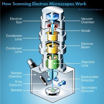
Figure 1- Overview of a scanning electron microscope (SEM)
The electron source (electron gun) is usually of thermionic emission type of filament or tungsten filament, but the use of field emission sources for higher resolution has increased. Usually, electrons are accelerated between 1-30 KeV. Then, two or three focusing lenses narrow the electron beam, to the extent that when it hits the sample, its diameter is about 2-10 nm.
The principles of SEM operation are based on three principles that are connected in a chain:
1.. The interaction of the electron beam with the sample;
2. The possibility of producing and controlling the characteristics of the scanning electron beam in electric and magnetic fields;
3. The possibility of detecting the rays emitted by the sample as a result of its interaction with the incoming electron beam.
When the scanning electron beam hits the sample, an interaction occurs between them. Its result is the emission of rays that are received and identified with the help of detectors and reveal the characteristics of the material.
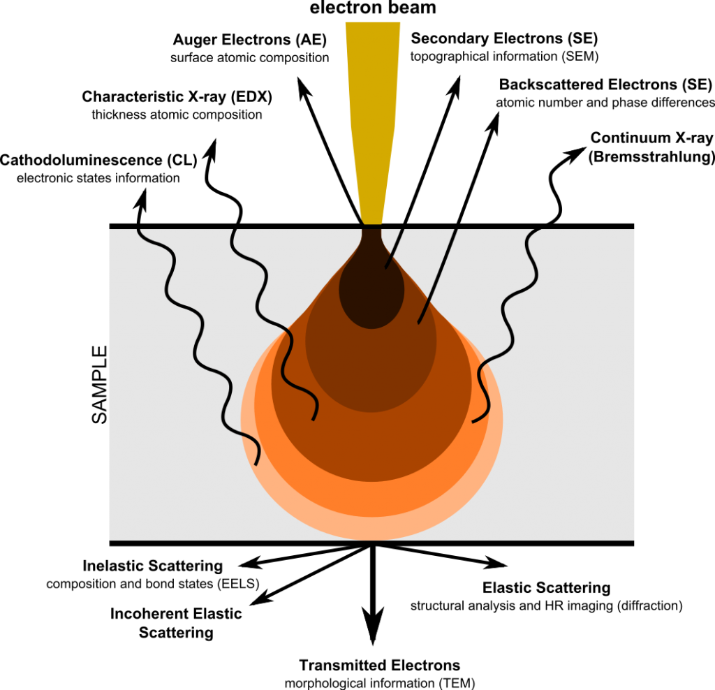
Figure 2- Interaction between electron beam and matter
applications
SEM is used in the study of many materials such as metals, alloys, magnetic materials, superconductors, semiconductors, ceramics, composites, bimetals, powders, ionic crystals, polymers, insulators, rubbers and plastics.
This research is in various branches such as crystal and grain growth, solidification, twin and crystalline directions, fracture, recovery, recrystallization, fatigue, corrosion, oxidation, wear, erosion, mechanical deformation, electrical connections, magnets, semiconductor components, electronic circuits and Covering is done. SEM analysis can provide information in the fields of morphology, topography, composition and crystallography.
Several examples of SEM applications include:
In addition to the mentioned cases, SEM also has many applications in nanotechnology, including measuring the size range of nanoparticles and examining their morphology, examining the structure of nanocomposites, the structure of nanotubes, the changes of nanostructures in different operations, nanofibers, nanostructure coatings, pharmaceutical nanostructures, He named nanofilters, the structure of nanoflowers, biological samples, and investigating phenomena and transformations at the nanoscale.
Advantages
The possibility of examining almost all types of samples (both conductive and non-conductive);
No need for transparent samples (due to the mechanism of action based on the interaction of the electron beam with the sample);
The possibility of imaging in three dimensions X, Y and Z
The possibility of communication and variety of results using different detectors;
Ease of working with the device despite proper training and computer improvements with special software;
the speed of working with the device;
Requires little initial preparation for most samples.
Limitations
Expensive, large and requiring an environment free of electrical, magnetic and vibrational interference;
low resolution, usually at more than a few tens of nanometers;
Black and white images due to the use of electron beam (however, in modern systems that are equipped with image analysis software, relatively colored images can be obtained by creating pseudo-color);
the need for high vacuum in the system;
The need for special training and experience to achieve excellent results and to detect misleading results (artifacts).
In most SEMs, samples are mounted on a sampler attached to a stand and enter the main chamber either directly or after passing through an intermediate chamber. The dimensions of the sample are limited according to the geometric dimensions of the chamber and the hardware equipment of the scanning and detection operations. There is this dimension limitation in X, Y and Z directions, of course, the amount of this limitation depends on the device model. Due to the dimensional limitation of the samples, there is usually a need to shrink the original samples.
Rigidity of the studied sample is another necessary property. Being solid is a necessary condition for being rigid, but not a sufficient condition. Due to the very strong suction that exists during the establishment of a vacuum in the chamber, in addition to the solidity of the sample, it is very important that the sample is dry and that no volatile substances, moisture, and types of fat are removed from the sample. The removal of these materials from the sample can contaminate the chamber, pores and ducts of the vacuum system and interfere with the path and scattering of electron beams.